Intel Ivy Bridge at IDF 2011
 Varghese George, senior principal engineer, has detailed information on the upcoming Ivy Bridge microarchitecture that’s due to be released in 1H 2012.
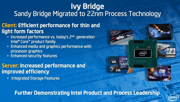
Ivy Bridge is the successor to incumbent Sandy Bridge – the design which powers the majority of Intel’s silicon available today – and it’s considered a tick in Intel’s nomenclature.
Ivy’s central core design is similar to Sandy Bridge in some ways, George said, as it features the same two-chip solution – PCH and CPU – socket, shared cache, and memory-controller found on the incumbent chip.
But George went on to explain that shifting down to 22nm and using the new-fangled tri-gate transistors enables Intel to offer either greater power efficiency or more performance than Sandy Bridge for a set die size, though he would not divulge actual numbers at the technical seminar at IDF.
While performance is clearly important for an architecture that will scale from ultra-low-voltage laptops through to servers, George was keen to point out that many of the improvements in Ivy Bridge relate to power efficiency. For example, new power-management features enable more-granular control over the chips’ cores and voltages, extending through to particular chips having multiple TDP settings that can be dynamically adjusted by a PC-manufacturing partner – a range of power settings on one chip, if you will. This intriguing notion was glossed over somewhat, and we plan to learn more tomorrow.
The time between Sandy and Ivy Bridge has enabled Intel to cook up a few new goodies with respect to performance, though. George indicated that Ivy Bridge parts have a collection of technologies for the core, cache and memory-controller that together boost the instruction-per-clock-cycle throughput. Again, no numbers or hard-and-fast data was shared.
Improvements in the instruction-set, new security features, and a boost in display outputs from the integrated graphics – from two to three – keep Ivy Bridge ticking along nicely, he concluded.
Supercharged graphics
Yet the biggest change in Ivy Bridge rests with the integrated graphics, offered Intel’s Tom Piazza. The graphics core is updated to support DX11 and all the necessary logic that it requires; faster QuickSync operation; a dedicated block for video encoding/decoding; and, now, a specific L3 graphics cache that’s not present in Sandy Bridge. It makes sense on this architecture as it’s potent enough to be able to actually use this cache in a meaningful way, Piazza remarked.
What’s unclear is whether these wholesale changes will enable Intel to compete with AMD’s impressive also-integrated graphics found on a range of Fusion chips. Only time will tell, we guess.
Something for the overclocker
Taking many design cues from Sandy Bridge means the new chips feature a tightly-coupled design. Helping out the overclocker, Intel’s board partners are to provide support for DDR3-2,800MHz memory (yes, you read that right), higher multiplier ratios on unlocked parts, and the ability to change said multipliers without rebooting the operating system.
In a nutshell
The Ivy Bridge microarchitecture is shaping up to be faster and more power-efficient than Sandy Bridge, clearly. There are no huge surprises here, and Intel’s bolstering of the graphics core is an obvious move.
We really need to see how the myriad of new technologies gel together before passing judgement, but such has been Sandy Bridge’s all-round excellence, fundamentally bettering it in every area is going to be an uphill task for 2012’s Ivy Bridge assortment of chips.
